08/20/19
This material complements section 2 – combinatorial logic design. I could not find any website with information about logic gates with PNP transistors; for our purposes, the following circuits work fine. As a general note, when using a voltage of around 5v to 6v, the resistance at the base of the transistor should be about 10kΩ, while the resistance of the emitter or collector should be about 1kΩ to 5kΩ. We’ll go over circuits that produce all the possible outputs for one and two inputs, with the exception of Xor and Xnor, for which we will devote a special section.
buffers
A buffer strengthens a signal without changing its logic value, i.e., if it receives a logic 1, it outputs a logic 1, and if receives a logic 0, it outputs a logic 0:
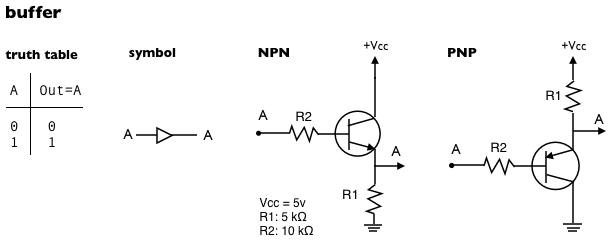
NPN and PNP buffers
Not gates
A Not gate is also called a negator, because it ‘negates’ (or toggles) the input, i.e., if it receives a logic 1, it outputs a logic 0, and if it receives a logic 0, it outputs a logic 1.
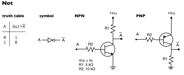
NPN and PNP Not gates
Notice that the NPN-based buffer and the PNP-based negator have the same configuration; the only difference is the transistor. Likewise, the PNP-based buffer and the NPN-based negator also have the same configuration. To go from one of these circuits to the other, all we need to do is replace the transistor with a complementary one. Complementary transistors use about the same power, we can trigger them with the same base currents, and their specs are such that the circuit that places one of the transistors in saturation places the other one in the cut-off region (see our previous tutorial on BJT transistors).
De Morgan’s laws
The De Morgan’s laws are two transformations of boolean expressions that allow us to express Or operations as And operations, and vice-versa. They are:
\[
A+B = \overline{\overline{A}\,\overline{B}}\\
AB = \overline{\overline{A}+\overline{B}}
\]
In the rest of this page we will find two-transistor circuits for many 2-input logic functions; these expressions are equal to their De Morgan-transformed expressions.
Series configurations
We connect transistors in series when we stack them one on top of the other, like battery cells in a flashlight.
NPN And gate
We can get an And gate using two NPN transistors connected in series in a common collector configuration:
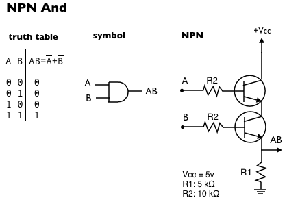
NPN And gate
PNP Nor gate
When we replace the NPN transistors of the And gate with PNP transistors, we get a Nor gate:
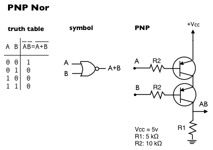
PNP Nor gate
0010 and 0100 series gates
A pair of NPN transistors in series gives us an And gate; a pair of PNP transistors in series gives us a Nor gate; what if we use one of each? Well… let’s see.
Normally we synthesize logic functions using a combination of standard gates; we can find buffers, Not’s, And’s, Or’s, Nand’s and Nor’s pre-packaged in integrated circuits (IC) chips like those of the 74xx series. We can build any logical output combining these standard gates. For example, suppose that we want the output to be 0010, i.e., we want the output to be a logic 1 only when the first input is 1 and the second is 0; logically speaking, we can achieve this output combining a Not and an And gate, and we can realize the circuit using a Not gate from a 7404 chip, and an And gate from a 7408:
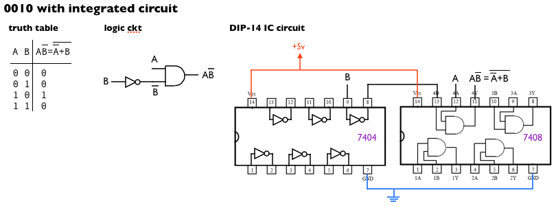
0010 integrated circuit
The 0001 output comes from a standard gate, i.e., the And function; the 0111 output also comes from a standard gate, i.e., the Or function. Both of them have electronic symbols too. However, the 0010 output does not come from a standard gate, and thus it does not have a name nor an electronic symbol.
The circuits that implement gates in ICs are more complex than the simple circuits that we are using in this page. The circuits in ICs address aspects like switching speed or fan-in. Still, suppose that we were to build the 0010 circuit that we built using ICs using our simple gates instead. If we use only NPN transistors, we would get something like this:
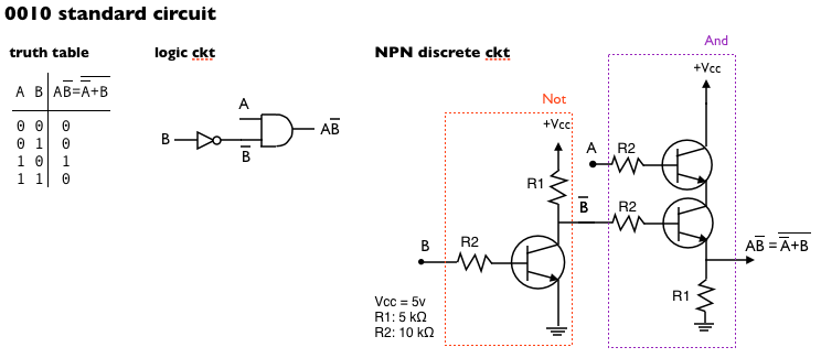
0010 standard gates
A straight mapping of the IC circuit to discrete gates requires three transistors: one for the Not gate and two for the And gate. The number of transistors in a circuit is proportional to the area that it occupies, the power that it consumes, and the heat that it produces, so in general, circuits with less transistors will take less space, consume less power, and produce less heat, all of which are desirable features.
Interestingly, though, if we are working with discrete transistors instead of ICs, we can build our 0010 function with only two transistors instead of three; here is where the combination of NPN and PNP transistors comes into play:
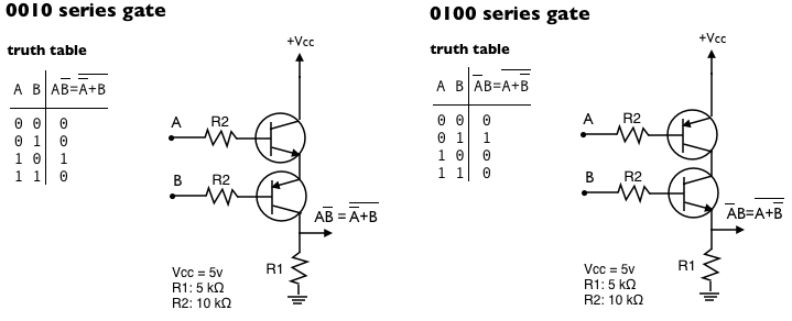
Changing the order of the stacking of the transistors of the 0010 circuit leads to the 0100, i.e., the circuits that produce 0010 and 0100 are electrically equivalent. However, being able to swap the order of the transistors gives us flexibility if we prefer one configuration over the other for wiring purposes.
All the series circuits above have in common that the output has exactly one logic 1 and three logic 0s; we decide which input combination will output the logic 1 changing the transistor type and their stacking order. We can put the circuit ‘upside-down’ and get circuits that produce, not a single logic 1 for a given input, but a single logic 0 for a given input. This is what we’ll work on next.
NPN Nand gate
We can get a Nand gate using two NPN transistors connected in series in a common emitter configuration:
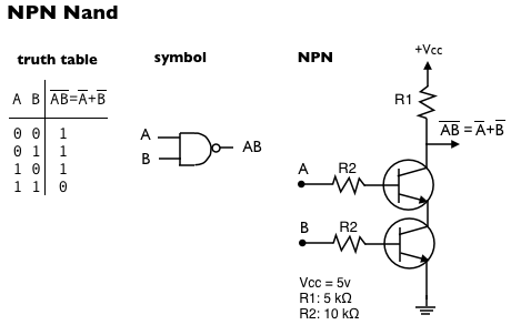
NPN Nand gate
PNP Or gate
When we replace the NPN transistors of the Nand gate with PNP transistors, we get an Or gate:
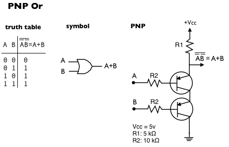
PNP Or gate
1101 and 1011 series gates
Replacing one of the NPN transistors of the Nand gate with a PNP transistor moves the output 0 to a different combination of inputs as follows:
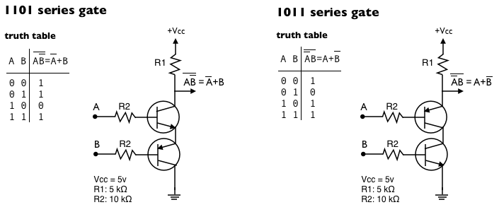
1101 and 1011 NPN and PNP circuits
Like the 0010 and 0100 circuits, the 1101 and 1011 are not standard and thus, they have no name or electronic symbols.
This concludes all the series configurations for two transistors. We found two-transistor circuits that generate the outputs 0001, 0010, 0100, 1000, 1110, 1101, 1011, and 0111. Now let’s find out what parallel configurations can do for us.
Parellel configurations
We connect transistors in parallel when we place them next to each other, like when we jump-start a car battery with another one.
We might be disappointed to learn that parallel configurations do not give us any new outputs. Instead, we obtain the same outputs that we obtained with the series configurations. However, they will become useful at the time when we need to combine series and parallel configurations.
NPN Or gate
Since we already described the gates, we will simply reiterate the De Morgan equivalences, the truth tables and point out the circuit:
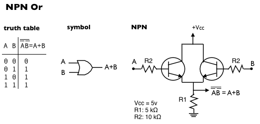
NPN Or gate
PNP Nand gate
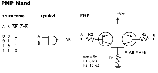
PNP Nand gate
1011 and 1101 parallel gates
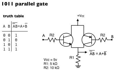
1011 parallel gate
and
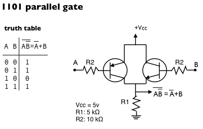
1101 parallel gate
NPN Nor gate
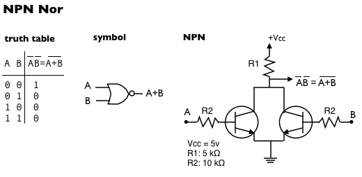
NPN Nor gate
PNP And gate
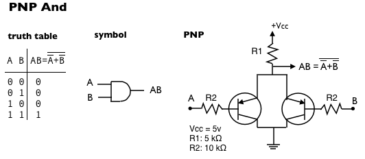
PNP And gate
0010 and 0100 parallel gates
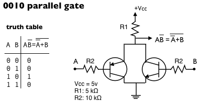
0010 parallel gate
and
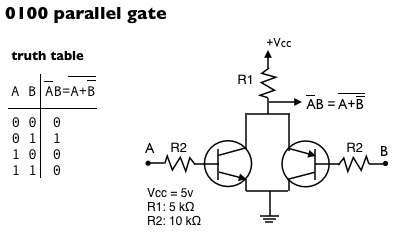
0100 parallel gate
Final comments
Usually there are many ways to solve a problem. Even with something as simple as finding a circuit that implements the 2-input-1-output logic functions described above, we have found solutions that use standard gates, series configurations, and parallel configurations. Most problems in life are the same: there are multiple solutions to any problem, and if we look carefully, we’ll find that some are better than others depending on the resources that we have at hand.
NPN and PNP transistors are two sides of the same coin. Whatever we can do with an NPN transistor, we can do with a PNP transistor. There are certain tradeoffs that have made NPN transistors a better choice for integrated circuit design. However, these tradeoffs have little to do with discrete element design. What we do not want to do is ignore possible solutions to a problem because we might have been blindsided to consider only solutions biased by the popularity of NPN designs, or constrained by the standardization of gates in chips.