08/19/19
This material supplements section 1 – circuits.
I’ll try to write something unusual each time I write one of these supplements. In this page, I describe a bare-bones model for the transistors, which has no use other than to make clear how an ideal transistor would replace a physical switch. In practice, even simple designs are likely to use standard transistor models that take into account voltage drops at the junctions, leaked currents, βs, and so on, but for us that have no background in electronics, our simple functional models are enough.
BJT transistors
There are several types of transistors; one of such types is called BJT (Bipolar Junction transistors). BJTs operate faster than most other types of transistors, but for our purposes, their particular advantage is that they are fairly resistant to static electricity, so we are less likely to damage them with the static electricity of our bodies, and we can handle them with our hands without having to be grounded; be aware that most other types of transistors are not so forgiving and touching them without being grounded are likely to damage them.
There are two types of BJTs: NPN (n-type/p-type/n-type) and PNP (p-type/n-type/p-type). An NPN transistor has two n-type semiconductor material sandwiching a p-type one; the PNP transistor is the reverse. The sandwiched region is called the ‘base’, while the regions on the sides are called the emitter and the collector.
In our lab circuits, we used 2N2222 transistors, which are NPN. NPN transistors have certain advantages at the time of designing integrated circuits, e.g., they are faster than PNP ones and use less silicon area. However, we are not designing an integrated circuit but instead working with discrete elements on a breadboard, so for that effect they are equivalent.
NPN and PNP transistors that have similar specs and operate in the same voltage range are called complementary. We are going to use the 2N2907 PNP transistor, which is a complementary PNP transistor for the NPN 2N2222 [wikipedia]. The spec sheets of these transistors are
Both the 2N2222A and the 2N2907 come in the same TO-92 package so they look the same; if our circuit is not working correctly, one of the first things to do it to make sure we are using the correct transistor.
This is the TO-92 package pin configuration of the two transistors:
2N2222A NPN and 2N2907 PNP pins in the TO-92 package
The two main purposes of a transistor are to amplify a signal, and to behave as a switch. When we use the transistor to amplify a signal, we configure it to operate in a region called the ‘active’ region. However, in logic design we only use the transistor as a switch, so we are only concerned with models and configurations of the transistor in which it behaves as an open switch, or a closed switch.
the transistor as a switch
Let’s start with an electrical switch that connects to points A and B. If we open the switch, the circuit is open and points A and B are physically disconnected – there is no path between them, so current cannot flow between them; if we close the switch, the circuit is closed and the points A and B are now physically connected – there is a path between them, so current can flow between them.
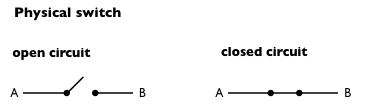
Physical switch – open and closed states
In a transistor, the emitter and the collector play the role of the switch terminals A and B, while the base controls the switch blade.
A transistor that is equivalent to an open switch is said to be in the ‘cut-off’ region. In an ideal model, a transistor in the cut-off region behaves as if it wasn’t there at all, opening the circuit in the same way that a physical switch would do, i.e., it is as if the points A and B were physically disconnected. Both the NPN and PNP transistors are in the cut-off region when their base currents are zero; there is no current in the base of an NPN transistor when we feed its base a logical 0, and there is no current in the base of a PNP transistor when we feed its base a logical 1. Remember that a logical 0 means a voltage close to 0v, while a logical 1 means, in our case, a voltage close to 5v.
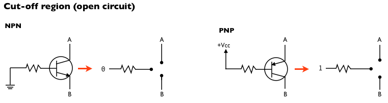
ideal behavior of NPN and PNP BJTs in the cut-off region
A transistor that is equivalent to a closed switch is said to be in the ‘saturation’ region. In an ideal model, a transistor in saturation behaves as if there was a wire between the emitter and the collector, closing the circuit in the same way that a switch blade in a physical switch would do, i.e., it is as if the points A and B were physically connected. Both the NPN and PNP transistors are in the saturation region when there is a current flowing through their bases; there is a current at the base of the NPN transistor when we feed the base a logical 1, and there is a current in the base of a PNP transistor when we feed the base a logical 0.
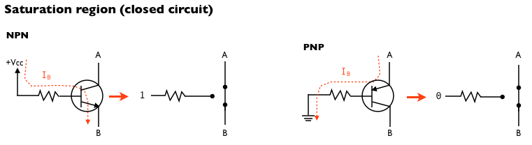
ideal behavior of NPN and PNP BJTs in the saturation region
The NPN and NPN transistors operate in opposite ways: the NPN transistor is in saturation when the base receives a logical 1, while the PNP is in saturation when the base receives a logical 0. In both cases, though, we place the transistor in saturation when we create a current that flows through both the emitter and the base of the transistor.
Although physically the base of a transistor is connected to the emitter and collector, our toy model shows the base always disconnected from the emitter and the collector. Remember that the job of a model is to describe how something works, not how something really is. In our model, we can think of the base as a remote control of a switch blade between points A and B.
Our models idealize the behavior of a transistor as a switch; if we decide to study electrical engineering, we will learn many transistor models that describe them more accurately, but for our purposes, our toy model suffices [transistor models].